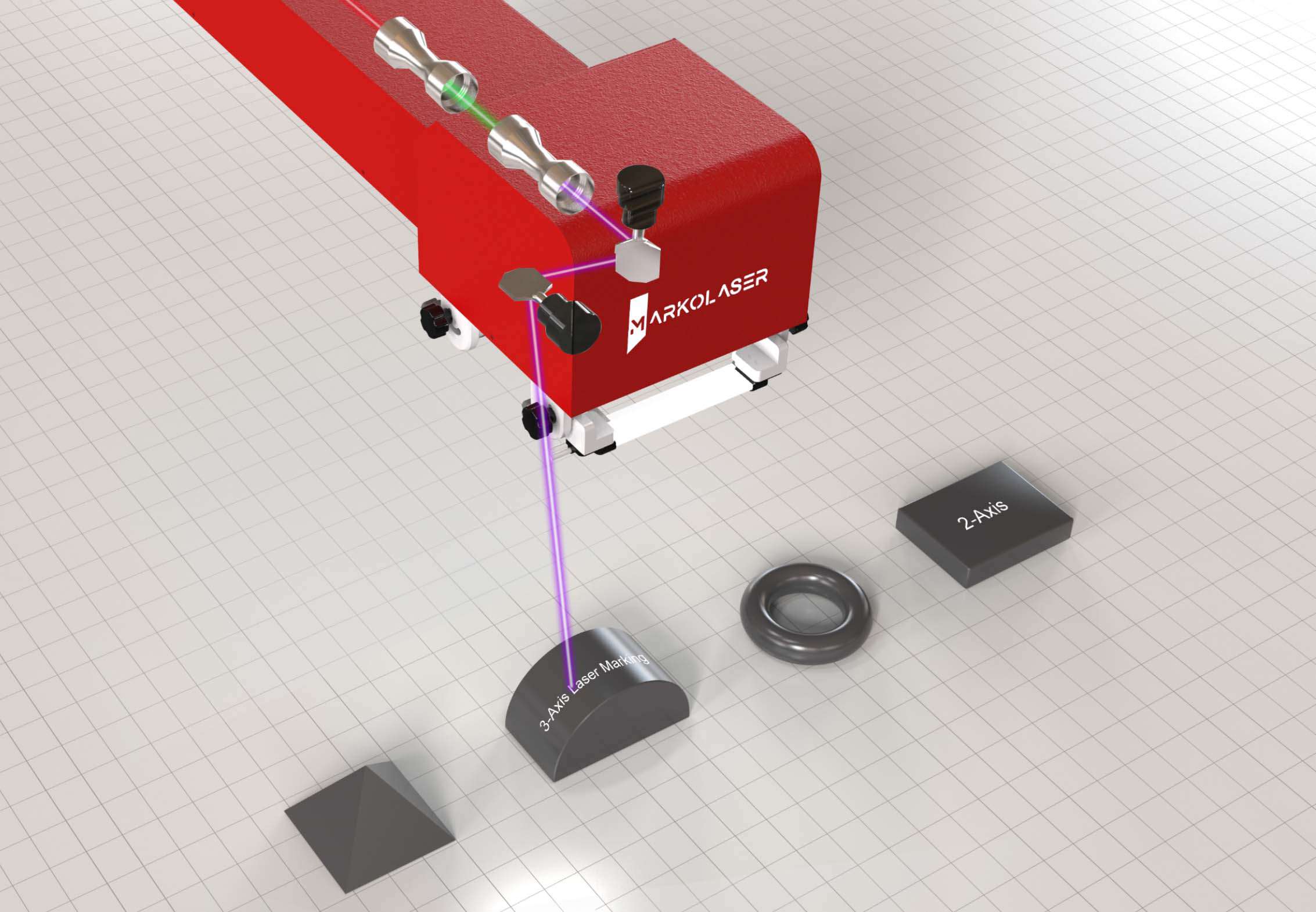
Distortion-free 3D/ 3-Axis Marking :
Our specialized 3D Lasers are well optically engineered to uniformly mark 3D shapes and surfaces.
The Laser marker can mark in the center as well as the edges of the object.
It won't distort 3D laser has the capability to mark any complex substrate and shape as per the requirement of the product. X Y Z Optical mechanism helps the laser to mark on any level on the surface of the metal or plastic with precision.
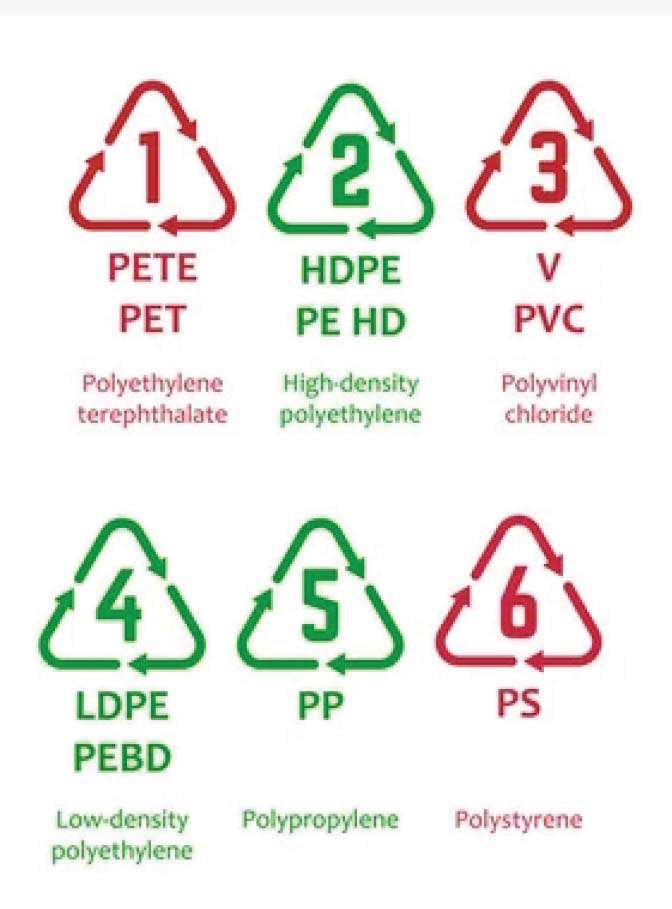
It could be any complex Plastic such as PP, ABS, PC(Nylon), PET. Moreover, marking on complex metals such as copper, brass, steel, iron, titanium, gold, silver, platinum, diamond is possible with our 3D Laser engraver/Marker.
High-speed 3D Laser for High productivity :
Markolasers High-Speed scanning system makes Markolasers system more substantial and more efficient to mark with consistency on any irregular surface or any substrate at any position with high speed. The Precise optical control of the laser marking head help in optimizing the field of marking area and the contrast of marking.
Conventional Laser Marker creates Distortion (i.e., you will get a fade/dim marked surface or non-marked product) and will not have the repeatability as 3X Laser Marker from the house of Markolaser.
Creating Value for OEMs with 3x Laser Marking Head for Traceability
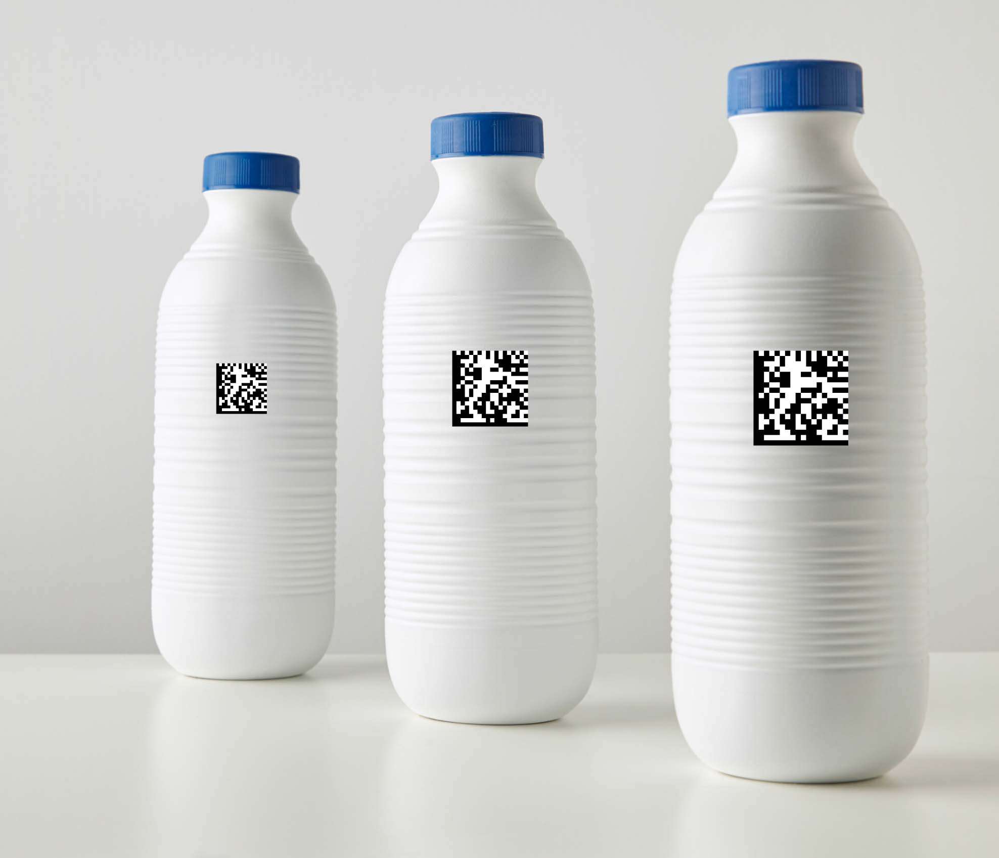
Improved laser marking options for traceability :
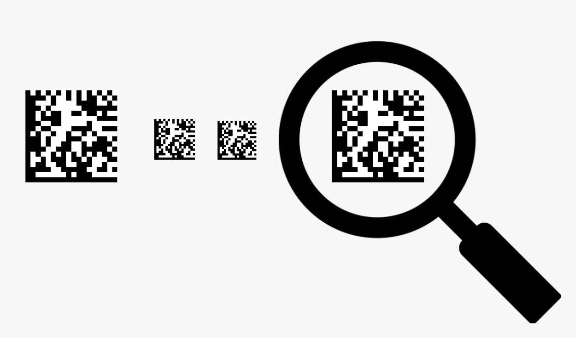
There is a demand for marking on a wider range of substrates for traceability in the industry. It is possible with UV 3axis laser marking, i.e., data matrix marking, Qr code marking, serialization.
Laser marking in a very small area with no distortion :
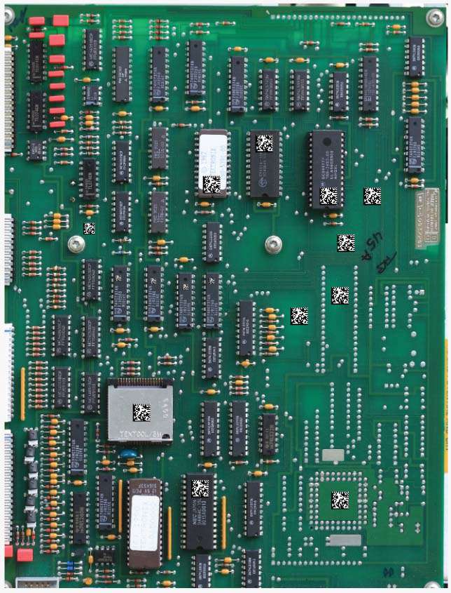
As the Semiconductor chip industry is growing, marking on an integrated chip has become the biggest requirement of the industry. Marking on a very small area with readability makes our laser the most demanding in the market. A damage-free marking and great flexibility to mark in a limited area make it the best and better in market..
Ability to mark with high-contrast on all difficult substrates:
Different resins have different strengths, and it's challenging to mark on various resins with a Normal wavelength laser. Once the wavelength deceases, the Laser beam gets finer and marking and controlling the laser beams easier.
This is the right time to use 3D UV Laser Marking System:
The future of the market is Semiconductor and PCB. The advancement of the Electronic industry and electronic household appliances and gadgets has given rise to the requirement of Semiconductor chips.
Laser Marking with our 3axis Laser marking system has made the life of electronics products manufacturing companies easy and better.
And manufacturing the PCB chip is not that easy. But, on the other hand, outsourcing them from other countries costs a lot to the countries such as India. Therefore governments of almost all the countries around the globe are concentrating on manufacturing their own PCB chips in-house.
Today the demand of the market is high-quality marking with the perfect contract. It is made easy with a Uv laser marker. However, it is achievable with Fiber laser markers also.
Now with the manufacturing of these chips. Traceability and laser marking application for serialization become an essential part of the product. We are ready to help these manufacturers with specialized Laser markers, customized and engineered as per the requirement of the electronic industry
3D Uv Laser Marker is the most sophisticated product as it works on the diverse substrate. Therefore, it has become more indispensable to select a versatile laser that is a thousand times better than any competitor in the market.
Definition of Cold Laser marking With UV Laser Engraver/Marker?
Laser marking in a very small area with no distortion :
Cold Laser Marking is defined as a marking with minimum heat stress that is only possible with a higher degree of absorption on varieties of the substrate.
Uv Laser Beam is the emission 3rd harmonic generation To understand it more technically, it is a process where a light beam is emitted at 1/3rd of the source wavelength.
Uv Laser Beam is generated after two-stage interaction The second harmonic beam is generated from the source laser in the first stage. After that, the second harmonic beam passes through the Sum-Frequency Generation stage, resulting in 3rd harmonics, i.e, UV Laser Beam.

UV Laser Marking Is also Called Damage Free Marking : Reason is that it Eliminates the Heat affected zone because of Cold UV Laser Marking
UDI Laser marking Surgical instrument (Steel)
.jpg)
Passivation free UDI Laser Marking : Minimal surface damage results in corrosion free engraving.
High contrast Laser marking on medical steel is only possible with Markolaser UDI marker.
Laser Marking and Cutting of Semiconductor PCB
Laser Marking and cutting is without thermal effects and breaks.
The Laser marking will not effect the circuit and its integrated component, Such as power diode, capacitor & inductor also known as passive component in electronics
3D Photonic Breakage and Damage with 353 nm Wavelength :
The Balanced laser energy of the UV Laser marking process results in photonic breakage of polymer bond at the molecular level. This Balanced wavelength of light reacts on the plastic surface (Semiconductor) in a unique manner. It doesn't lead to the heat affect zone, thus minimizing the burn or damage.
3 Axis Laser to Minimize Surface Damage on Metals:
Our UV laser marker has a wow effect with all the metals as well as precious metals such as gold, silver, copper, brass, bronze. Etc. It reacts best with diamond & ceramic non-metallic products. In the case of a highly reflective surface, our UV laser reduces burrs and soot, thus not affecting the metal's surface. We can also call it corrosion-free marking.
